
The most commonly used transmission lines (stripline and microstrip line) aren't the only way to transmit a signal from one place to another. Having a variety of transmission lines in your tool kit can get you out of trouble in tricky situaTIons. This arTIcle describes some useful transmission lines and the problems they solve.
Guiding the WaveMicrowave signals are transmitted from locaTIon-to-location by waveguides or antennas. The chief difference between the two is that a waveguide confines the electromagnetic field to an area along the path, while an antenna radiates the electromagnetic field into space. In a waveguide, radiation is bad. In an antenna, radiation is the goal.
A transmission line is a sub-category of waveguides that uses some physical configuration of metal and/or dielectrics to direct a signal along the desired path. Most familiar transmission lines (e.g., microstrip line) use two conductors; signal and ground, however, there are single conductor transmission lines (e.g., rectangular waveguide).
For analysis, we want to be able to predict two important parameters of a transmission line: the characteristic impedance and the electrical length. Knowing these allows you to easily simulate or calculate circuit performance. These parameters can be obtained from closed-form equations, numerical approximations, and 2-D, 2½-D, or 3-D electromagnetic simulations. Closed-form equations are great for intuition and analyses with spreadsheets like Microsoft Excel. A good source for these equations is the Transmission Line Design Handbook.
The Simplest Transmission Line - Coaxial LineThe simplest transmission line configuration is coaxial line. It is simple because a there is an exact solution for its impedance and propagation velocity in terms of the physical parameters (conductor sizes). Equations for many transmission line types have been derived by mapping their physical shape into a coaxial shape where the solution is known exactly. 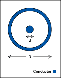
Figure 1. Coaxial line can be useful rven in planar circuits.
You might think that coaxial lines are not useful in printed-circuit board design because they are not planar. However, there are a couple of places you may want to use the coaxial line.
The first situation is encountered when routing a signal through the printed circuit board. Passing from one layer of the printed-circuit board to another is done with round pads on each layer and holes that are plated with metal to connect these pads. The pad for the via is surrounded by a ground plane. The pad and its surrounding ground plane cut-out form a very short section of coaxial transmission line. You can use coaxial line equations to match these transmission lines to the surrounding circuitry and thus minimize the discontinuity.
Very small coaxial lines are available in semi-rigid form having quite small outer diameters - down to 0.2mm (0.008in.). These coaxial lines are a perfect way to provide a fully shielded path for signals on printed-circuit boards in low volume production, as rework, and for prototyping. Sizes around 0.5mm (0.020in.) bend readily and are easy to cut and strip with an Exacto knife. Just trim the ends and solder the shield to the ground plane.
The Stripline FamilyStripline was invented by flattening the coaxial line configuration. It has also been called Triplate or sandwich line. The presence of both top and bottom shields provides good isolation from other signals on the printed-circuit board.
Some useful forms of stripline include centered stripline in Figure 2, off-center stripline in Figure 3, and dual orthogonal stripline in Figure 4. Centered stripline is the ideal situation, however layout decisions may require an off-center stripline. The dual orthogonal stripline configuration is useful in high density routing situations and is accomplished by routing two off-center layers at right angles to each other.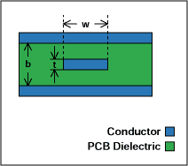
Figure 2. Centered stripline.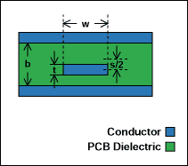
Figure 3. Off-center stripline.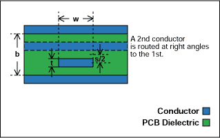
Figure 4. Dual orthogonal stripline.
The Microstrip Line FamilyThe microstrip line simplifies the stripline by removing the upper ground planes. It is probably the most popular planar transmission line because of its ease of fabrication and the ready availability of the signals for probing and circuit connections. Its disadvantage over stripline is that some of the energy transmitted may be coupled into space or adjacent traces. 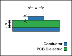
Figure 5. Microstrip line.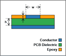
Figure 6. Embedded microstrip line.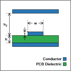
Figure 7. Covered microstrip line.
The most useful configurations for designers are microstrip line shown in Figure 5, embedded microstripline shown in Figure 6, and covered microstrip line shown in Figure 7. Embedded microstrip line is the situation encountered when the microstrip line is covered with solder mask or a thin layer of epoxy. Covered microstrip line is a transitional structure somewhere between microstrip line and stripline. When an electrically close shield covers the circuit you will want to analyze it as a covered microstrip line.
The Coplanar Waveguide FamilyAll of the transmission lines so far scale the signal conductor's dimensions to the separation of the ground conductor to set the impedance. Once you choose the dielectric thickness the other dimensions are determined. Sometimes this can be inconvenient when connecting to other components.
For example, when you need to transition to a connector or device pin that has a specific pin size, the trace width may turn out to be too wide to fit between pins. You could taper the dielectric substrate thickness to allow the signal conductor's width to narrow but that is usually impractical. Fortunately, the coplanar waveguide family solves this problem. 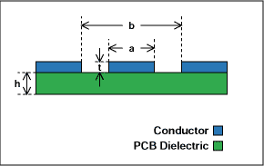
Figure 8. Coplanar waveguide.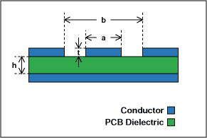
Figure 9. Coplanar waveguide with ground.
Coplanar waveguide (CPW) uses a ground conductor that is coplanar with the signal conductor. Therefore, the impedance is controlled by the signal line width and the ground gap. What this means is that you can keep the impedance constant as you taper the signal conductor's width down to meet a pin. This is perfect for matching to a component pin width without changing the substrate thickness!
The coplanar waveguide configurations that are most likely to be useful are: coplanar waveguide and coplanar waveguide with ground. Coplanar waveguide concentrates the field in the gap so it will have the best ability to taper in to a pin. However, it may require special attention if you are transitioning from microstrip line into CPW. In this situation, coplanar waveguide with ground (CPWG) may be easier to deal with since you can start with a wide gap (microstripline) and gradually transition to the coplanar waveguide with ground configuration.
ConclusionYou do not have to limit your designs to microstrip lines and striplines. Transmission lines, such as coaxial line, shielded microstrip line, and the coplanar waveguide family, can help designers solve real world layout problems while maintaining tight control of the waveguide characteristic impedance and physical dimensions.
1. Transmission Line Design Handbook, by Brian C. Wadell, ISBN 0-89006-436-9, published by Artech House.
欢迎分享,转载请注明来源:内存溢出

 微信扫一扫
微信扫一扫
 支付宝扫一扫
评论列表(0条)